This is the official manual. Enjoy!
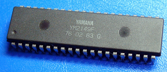
Yamaha YM2149
Software-Controlled Sound Generator (SSG)
Overview
The SSG (Software-Controlled Sound Generator) is an NMOS-LSI device designed to be capable of music generation. It only requires the microprocessor or microcomputer (CPU) to initialize its register array, thus reducing the load on the CPU. Music generation is carried out by the three sequence square wave generator, noise generator, and envelope generator according to the set parameters. This allows for the generation of music, special effects, warnings, and various other types of sounds.
Features
- 5V single power supply
- Easy connection to 8 bit or 16 bit CPU
- Simple connection to external system through 2 sequence 8 bit I/O port
- Wide voicing range of 8 octaves
- Smooth attenuation by 5 bit envelope generator
- Built-in 5 bit D/A convertor
- Input of double frequency clock can be handled by built-in clock frequency divider
- TTL compatible level
- Low power consumption (typical 125mW)
- 40 pin plastic DIL package
- Pin compatible with AY-3-8910 manufactured by GI
Pin Layout
        Vss(GND) 1          40 Vcc(+5V)
             N.C 2          39 Test1
Analog Channel B 3          38 Analog Channel C
Analog Channel A 4          37 DA0
             N.C 5          36 DA1
            IOB7 6          35 DA2
            IOB6 7          34 DA3
            IOB5 8          33 DA4
            IOB4 9          32 DA5
           IOB3 10          31 DA6
           IOB2 11          30 DA7
           IOB1 12          29 BC1
           IOB0 13          28 BC2
           IOA7 14          27 BDIR
           IOA6 15          26 SEL
           IOA5 16          25 A8
           IOA4 17          24 A9
           IOA3 18          23 RESET
           IOA2 19          22 CLOCK
           IOA1 20          21 IOA0
Block diagram
  A9 A8     BDIR BC2 BC1          DA7~DA0
   o o        o   o   o             |
   | |        |   |   |             |
   | |        |   |   |             |
   | |   --- Bus Control ---o  Bidirectional      -----o I/O Port A <=> IOA7~IOA0
   | |   |    Decoder    o---     buffer          |
   | |   |                          o             |
   | |   |                          |             |
   | |   o                          o             |
   Register Addr --o Address --o Register o-------|
      Latch          Decoder      Array           -----o I/O Port B <=> IOB7~IOB0
                                    o
                                    |
       --------------------------------------
       |          |     |     |             |
       o          o     |     o             o
     Noise      Music   |  Envelope       Level         Frequency
   Generator  Generator |  Generator --o Control o-----  divider  ---o CLOCK
       |          |     |                   |   master      |
       |          o     |                   |    clock      |
       -------o Mixer o--                   |               ---------o SEL
                  |                         |
                  |                         |
                  o                         |
           D/A Convertor o------------------
             |    |    |
             |    |    |
            Analog Channel
             o    o    o
             A    B    C
Description of pins
- DA7 ~ DA0
This is an 8 bit bidirectional data bus which is used for moving data and addresses between the SSG and CPU. In the read and write modes, DA7 ~ DA0 corresponds to B7 ~ B0 of the register array. In the address mode, DA3 ~ DA0 is used for the register address, and DA7 ~ DA4 is used together with A9 and A8 for the upper address. - A8 and A9
These are the upper address input pins. A8 has pullup resistance while A9 has pulldown resistance. When the voltage level at A8 while the level at A9 and DA7 ~ DA4 is low, the address mode is selected allowing for the fetching of a register address. Connect A8 and A9 to +5V and ground respectively when not in use. - RESET
Reset is effective when the voltage level is low, and the contents of all registers in the array are reset to ‘0’. This pin has pullup resistance. - CLOCK
Supplies the master clock to the sound generator and envelope generator. This is equipped with a 1/2 frequency divider which allows for the use of a frequency which is 1/2 of the input clock, as the master clock. - SEL
When SEL is driven to the high level, the input clock is taken as the master clock. When the voltage level of SEL is low, the input clock is divided by 2 to obtain the master clock. This pin has pullup resistance, allowing for full pin compatibility with the AY-3-8910 manufactured by AI, when this pin is not connected to anything. - BDIR,BC1 and BC2
Controls the external bus (DA7 ~ DA0) and internal bus of the SSG. The following four modes can be set by the bus control decoder. The bus control is redundant, control is possible even when BC5 is connected to +5V.
 BDIR BC2 BC1   Mode
   0   0   0    Inactive
   0   0   1    Address
   0   1   0    Inactive
   0   1   1    Read
   1   0   0    Address
   1   0   1    Inactive
   1   1   0    Write
   1   1   1    Address
Inactive mode: DA7 ~ DA0 has high impedance.
Address mode: DA7 ~ DA0 set to input mode, and address is fetched from
register array.
Write mode: DA7 ~ DA0 set to input mode, and data is written to register
currently being addressed.
Read mode: DA7 ~ DA0 set to output mode, and contents of register
currently being addressed are output.
7. ANALOG CHANNEL A,B,C
Each of the three channels is equipped with a D/A convertor which converts
the calculated digital values to analog signals for output.
8. IOA7 ~ IOA0, IOB7 ~ IOB0
These are two 8 bit I/O ports. These ports allow the SSG to be placed
between an external system and the CPU for the transfer of data. These pins
have pullup resistance.
9. TEST1
Output pin for testing the device. Do not connect to anything.
10. Vcc
+5V power pin.
11. Vss
Ground pin.
Description of funtions
All functions of the SSG are controlled by the 16 internal registers. The CPU need only write data to the internal registers of the SSG. The SSG itself generates the sound. Sound is generated by the following blocks:
- Music generator: Square waves having a different frequency are generated for each channel (A,B and C)
- Noise generator: Pseudo-random waveforms are generated (variable frequency)
- Mixer: Music and noise output are mixed for the three channels (A,B and C)
- Level control: Constant level or variable level is given for each of the three channels (A,B and C). Constant levels are controlled by the CPU, and variable levels by the envelope generator.
- Envelope generator: Generates various types of attenuation (single burst attenuated and repeated attenuation)
- D/A convertor: Sound is output on each of the three channels (A,B and C) at the level determined by the level control.
The CPU can read the contents of the internal registers with no effect on sound.
Register Array

 A9  A8 DA7 DA6 DA5 DA4 DA3 DA2 DA1 DA0
 0   1   0   0   0   0   0   0   0   0
 0   1   0   0   0   0   1   1   1   1
\______________________/\_____________/
     Upper addresses    Lower addresses
      (chip select)    (register select)
Of the ten bit address, the lower addresses DA3 ~ DA0 are used to select the 16 internal registers(register array). The upper addresses are used for chip selection. A9 and A8 is programmed to 01 while DA7 through DA4 are set to 0000. When the upper addresses match this program in the address mode, a register address (lower four bits DA3 through DA0) is fetched from the register address latch. When the value set is in the upper addresses is different from the program value, the bidirectional bus formed from DA7 through DA0 is driven to high impedance. A register address which has been fetched is retained until the next address is fetched, and is not affected by the read, write, or inactive mode.
  Register Array
                            B7....B0
R0 Frequency of Channel A   00000000   8 bit fine tone adjustment
R1                          ----0000   4 bit rough tone adjustment
R2 Frequency of Channel B   00000000   8 bit fine tone adjustment
R3                          ----0000   4 bit rough tone adjustment
R4 Frequency of Channel C   00000000   8 bit fine tone adjustment
R5                          ----0000   4 bit rough tone adjustment
R6 Frequency of Noise       ---00000   5 bit noise frequency
R7 I/O port and mixer       iinnnttt   i-I/O, n-Noise, t-Tone
   settings                 bacbacba
R8 Level of channel A       ---mllll   m-Mode, l-Level
R9 Level of channel B       ---mllll   m-Mode, l-Level
RA Level of channel C       ---mllll   m-Mode, l-Level
RB Frequency of envelope    00000000   8 bit fine adjustment
RC                          00000000   8 bit rough adjustment
RD Shape of envelope        ----cath   c-Cont, a-Att, t-Alt, h-Hold
RE Data of I/O port A       00000000   8 bit data
RF Data of I/O port B       00000000   8 bit data
(1) Setting of music frequency (controlled by registers R0 ~ R5)
The frequencies of the square wave generated by the music generators for the three channels (A,B and C) are controlled by registers R0 through R5. R0 and R1 control channel A, R2 and R3 are used for channel B, and R4 and R5 control channel C. The oscillation frequency fT is obtained in the following manner from the value of the register TP(decimal).
   fT = fMaster
        -------
         16TP
fMaster is the frequency of the master clock (this is the input click frequency when SEL is high, and 1/2 of this frequency when low).
Rough tone adjustment                 Fine tone adjustment
      register           Channel           register
         R1                 A                 R0
         R3                 B                 R2
         R5                 C                 R4

B7 B6 B5 B4 B3 B2 B1 B0           B7 B6 B5 B4 B3 B2 B1 B0
\---------/|            \       /
 Not used  |              \   /
           |                |
           TP11 TP10 TP9 TP8 TP7 TP6 TP5 TP4 TP3 TP2 TP1 TP0
            12 bit oscillation frequency setting value (TP)
(2) Setting of noise generator (controlled by register R6)
The noise frequency fN is obtained from the register value NP(decimal) in the following manner.
   fN = fMaster        (fMaster if the frequency of the master clock)
        -------
         16NP
  Noise frequency register R6
    B7 B6 B5 B4 B3 B2 B1 B0
    \------/|               \
    Not used|                \
            |                 |
            NP4 NP3 NP2 NP1 NP0
     5 bit noise frequency setting value (NP)
(3) Settings of mixer and I/O ports (controlled by register R7)
The mixer is used to combine music and noise components. The combination is determined by bits B5 ~ B0 of register R7. Sound is output when a ‘0’ is written to the register. Thus, when both the noise and tone are ‘0’, the output is combined by the mixer. When the noise is ‘0’ and the tone is ‘1’, only the noise signal is output. When the noise is ‘1’ and the tone is ‘0’, music (square wave) is output. Nothing is output when both the noise and tone are ‘1’. Selection of input/output for the I/O ports is determined by bits B7 and B6 of register R7. Input is selected when ‘0’ is written to the register bits.
  I/O port and mixer setting register R7
        B7 B6 B5 B4 B3 B2 B1 B0
      /     /|        |\        \
    /     /  |        |  \        \
     I/O       Noise        Tone
    B   A     C   B   A    C   B   A
(Input is selected for I/O port when ‘0’, and noise or tone can be output when ‘0’)
(4) Level control (controlled by R8 ~ RA)
The audio level output from the D/A convertors for the three channels (A,B and C) is adjusted by registers R8, R9 and RA.
    Level setting registers  Channel
             R8                 A
             R9                 B
             RA                 C

        B7 B6 B5 B4 B3 B2 B1 B0
        \------/|  |\          \
        Not used|  |  \          \
                |  |    \          \
                 M        L3 L2 L1 L0
                Mode   4 bit level selection
Mode M selects whether the level is fixed (when M=0) or variable (M=1). When M=0, level is determined from one of 16 by level selection signals L3,L2,L1 and L0 which compromise the lower four bits. When M=1, the level is determined by the 5 bit output of E4,E3,E2,E1 and E0 of the envelope generator of the SSG. (This level is variable as E4 ~ E0 change over time)
(5) Setting of envelope frequency (controlled by R8 and RC)
Thus, the envelope repetition frequency fE is obtained as follows from the envelope setting period value EP (decimal):
   fE = fMaster        (fMaster if the frequency of the master clock)
        -------
         256EP
Envelope rough adjustment register RC  Envelope fine adjustment register RB
        B7 B6 B5 B4 B3 B2 B1 B0           B7 B6 B5 B4 B3 B2 B1 B0
      /                         \       /                         \
    /                             \   /                             \
  /                                 |                                \
  EP15 EP14 EP13 EP12 EP11 EP10 EP9 EP8 EP7 EP6 EP5 EP4 EP3 EP2 EP1 EP0
                16 bit envelope period setting value (EP)
The period of the actual frequency fEA used for the envelope generated is 1/32 of the envelope repetition period (1/fE).
(6) Envelope shape control (controlled by RD)
The envelope generator counts the envelope clock fEA 32 times for each envelope pattern cycle. The envelope level is determined by the 5 bit output (E4 ~ E0) of the counter. The shape of the envelope is created by increasing, decreasing, stopping, or repeating this counter. The shape is controlled by bits B3 ~ B0 of the register RD.
  Envelope shape control register RD
        B7 B6 B5 B4 B3 B2 B1 B0
        \----------/ |  |  |  |
          Not used   |  |  |  --- Hold
                     |  |  ------ Alt
                     |  --------- Att
                     ------------ Cont
                Envelope shape control signals
The envelope can take the shapes shown below according to combinations of the CONT, ATT, ALT and HOLD signals.
       B3  B2  B1   B0
      CONT ATT ALT HOLD
        0   0   x   x  \
                        \---------------------

        0   1   x   x   /|
                       / |--------------------

        1   0   0   0  \ |\ |\ |\ |\ |\ |\ |\
                        \| \| \| \| \| \| \| \

        1   0   0   1  \
                        \---------------------

        1   0   1   0  \  /\  /\  /\  /\  /\  /
                        \/  \/  \/  \/  \/  \/

        1   0   1   1  \ |--------------------
                        \|

        1   1   0   0   /| /| /| /| /| /| /| /
                       / |/ |/ |/ |/ |/ |/ |/

        1   1   0   1   /---------------------
                       /

        1   1   1   0   /\  /\  /\  /\  /\  /\
                       /  \/  \/  \/  \/  \/  \

        1   1   1   1   /|
                       / |--------------------
NOTE - The writing to register RD will reset the envelope frequency.